SOURCE // srambc1.mag
PDK // SKY130A · DRC // CLEAN
← ProjectsP-03 · Silicon

6T SRAM Bitcell

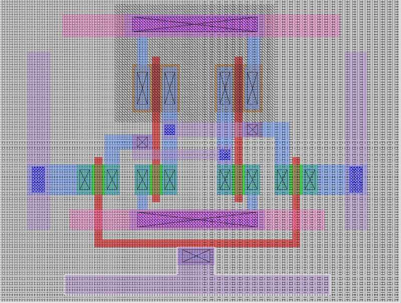
A full-custom, transistor-level layout of a six-transistor static RAM cell, drawn by hand in Magic VLSI on the open-source SkyWater 130nm process.

MAGIC VLSISKYWATER 130NMNGSPICECUSTOM LAYOUTDRC CLEAN
SCROLL TO EXPLORE
SCROLL — 7 CHAPTERS
02
Under the hood

The details

Circuit

Two cross-coupled CMOS inverters (M1–M4) form a bistable latch that stores the bit on nodes Q and QB. Two NMOS access transistors (M5, M6), gated by the wordline, connect those nodes to the bitlines BL and BLB.

        VDD                 VDD
         │                   │
       [M2] PMOS           [M4] PMOS
 BL      │     Q     QB      │      BLB
  │──[M5]┤──────┐ ┌──────├[M6]──│
  │      │      └─┼─┐    │      │
       [M1] NMOS  │ │  [M3] NMOS
         │        WL         │
        GND                 GND

Sizing rules

Read stability — cell ratio. Pull-down (M1, M3) over access (M5, M6) is kept above about 1.2–1.5, so a read never lifts the stored-0 node past the opposite inverter's trip point.

Writeability — pull-up ratio. Pull-up (M2, M4) over access is kept below 1.0, so the access transistor can pull the node down against the PMOS during a write.

Flow

Drawn in Magic VLSI on the SkyWater 130nm PDK, 100% DRC clean. The netlist is extracted with ext2spice and simulated in Ngspice.

6T SRAM bitcell layout in Magic VLSI
Layout in Magic VLSI — hover for colourSRAMBC1.MAG